- 您现在的位置:买卖IC网 > Sheet目录476 > MCH6431-TL-H (ON Semiconductor)MOSFET N-CH 30V 5A MCPH6
MCH6431
Electrical Characteristics at Ta=25°C
Parameter
Symbol
Conditions
min
Ratings
typ
max
Unit
Drain-to-Source Breakdown Voltage
Zero-Gate Voltage Drain Current
Gate-to-Source Leakage Current
V(BR)DSS
IDSS
IGSS
ID=1mA, VGS=0V
VDS=30V, VGS=0V
VGS=±16V, VDS=0V
30
1
±10
V
μ A
μ A
Cutoff Voltage
Forward Transfer Admittance
VGS(off)
| yfs |
RDS(on)1
VDS=10V, ID=1mA
VDS=10V, ID=2.5A
ID=2.5A, VGS=10V
1.2
2.2
42
2.6
55
V
S
m Ω
Static Drain-to-Source On-State Resistance
Input Capacitance
Output Capacitance
Reverse Transfer Capacitance
Turn-ON Delay Time
Rise Time
Turn-OFF Delay Time
Fall Time
Total Gate Charge
Gate-to-Source Charge
Gate-to-Drain “Miller” Charge
Diode Forward Voltage
RDS(on)2
RDS(on)3
Ciss
Coss
Crss
td(on)
tr
td(off)
tf
Qg
Qgs
Qgd
VSD
ID=1.2A, VGS=4.5V
ID=1.2A, VGS=4V
VDS=10V, f=1MHz
See speci ? ed Test Circuit.
VDS=15V, VGS=10V, ID=5A
IS=5A, VGS=0V
65
78
280
60
30
5.7
11
21
10
5.6
1.2
0.8
0.85
91
109
1.2
m Ω
m Ω
pF
pF
pF
ns
ns
ns
ns
nC
nC
nC
V
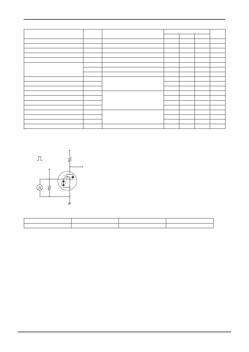
Switching Time Test Circuit
VDD=15V
10V
0V
VIN
ID=2A
RL=7.5 Ω
PW=10 μ s
D.C. ≤ 1%
VIN
D
VOUT
G
P.G
50 Ω
S
MCH6431
Ordering Information
Device
MCH6431-TL-H
Package
MCPH6
Shipping
3,000pcs./reel
memo
Pb Free and Halogen Free
No. A1852-2/7
发布紧急采购,3分钟左右您将得到回复。
相关PDF资料
MCH6436-TL-E
MOSFET N-CH 30V 6A MCPH6
MCH6437-TL-E
MOSFET N-CH 20V 7A MCPH6
MCH6444-TL-H
MOSFET N-CH 35V 2.5A MCPH6
MCH6445-TL-E
MOSFET N-CH 60V 4A MCPH6
MCH6448-TL-H
MOSFET N-CH 20V 8A MCPH6
MCH6602-TL-E
MOSFET N-CH DUAL 30V 350MA MCPH6
MCH6604-TL-E
MOSFET N-CH DUAL 50V 250MA MCPH6
MCH6613-TL-E
MOSFET N/P-CH 30V 350MA MCPH6
相关代理商/技术参数
MCH6436
制造商:SANYO 制造商全称:Sanyo Semicon Device 功能描述:General-Purpose Switching Device Applications
MCH6436_12
制造商:SANYO 制造商全称:Sanyo Semicon Device 功能描述:General-Purpose Switching Device Applications
MCH6436-TL-E
功能描述:MOSFET SWITCHING DEVICE RoHS:否 制造商:STMicroelectronics 晶体管极性:N-Channel 汲极/源极击穿电压:650 V 闸/源击穿电压:25 V 漏极连续电流:130 A 电阻汲极/源极 RDS(导通):0.014 Ohms 配置:Single 最大工作温度: 安装风格:Through Hole 封装 / 箱体:Max247 封装:Tube
MCH6437
制造商:SANYO 制造商全称:Sanyo Semicon Device 功能描述:General-Purpose Switching Device Applications
MCH6437_12
制造商:SANYO 制造商全称:Sanyo Semicon Device 功能描述:General-Purpose Switching Device Applications
MCH6437-P-TL-E
功能描述:MOSFET RoHS:否 制造商:STMicroelectronics 晶体管极性:N-Channel 汲极/源极击穿电压:650 V 闸/源击穿电压:25 V 漏极连续电流:130 A 电阻汲极/源极 RDS(导通):0.014 Ohms 配置:Single 最大工作温度: 安装风格:Through Hole 封装 / 箱体:Max247 封装:Tube
MCH6437-TL-E
功能描述:MOSFET SWITCHING DEVICE RoHS:否 制造商:STMicroelectronics 晶体管极性:N-Channel 汲极/源极击穿电压:650 V 闸/源击穿电压:25 V 漏极连续电流:130 A 电阻汲极/源极 RDS(导通):0.014 Ohms 配置:Single 最大工作温度: 安装风格:Through Hole 封装 / 箱体:Max247 封装:Tube
MCH6438
制造商:SANYO 制造商全称:Sanyo Semicon Device 功能描述:P-Channel Silicon MOSFET General-Purpose Switching Device Applications
